

This technology cluster will enable the fabrication of large area photonic and optoelectronic structures, devices and systems. On the one hand, printing and coating technologies will be used to deposit large area functional layers by fast and low-cost methods. We will install possibilities for large area deposition as well as for highly resolved digital printing.
On the other hand, we will establish patterning and replication technologies for light management and surface modification. Suitable large area nano- and micro-structures are of key importance for several applications. Anti-reflection coatings and in-coupling of light into detectors, sensors and solar cells – and vice versa the out-coupling of light from lightemitting devices – play a pivotal role for the overall efficiency of optoelectronic devices and systems. The possibility of large area patterning and tailoring optical properties will also offer novel approaches for biophotonics.
Technologies
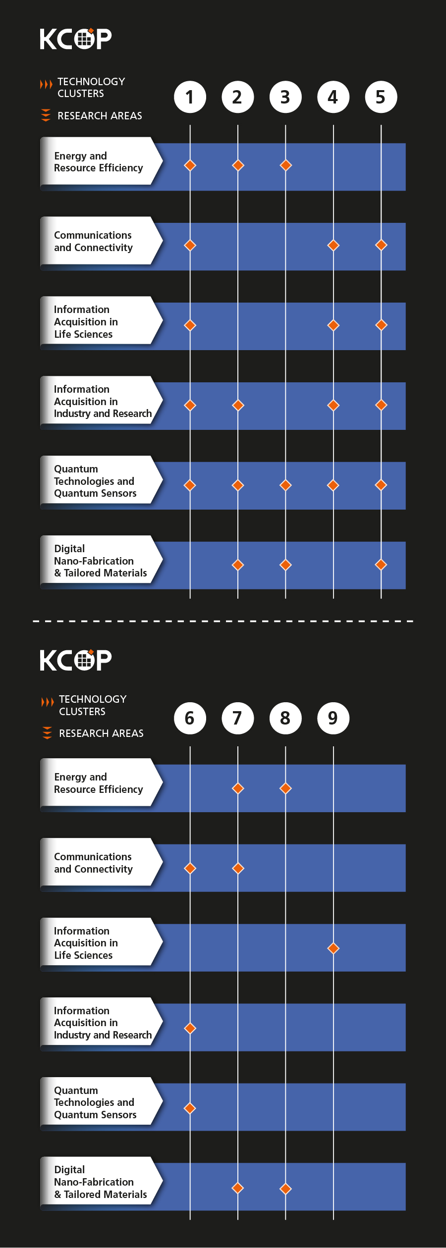
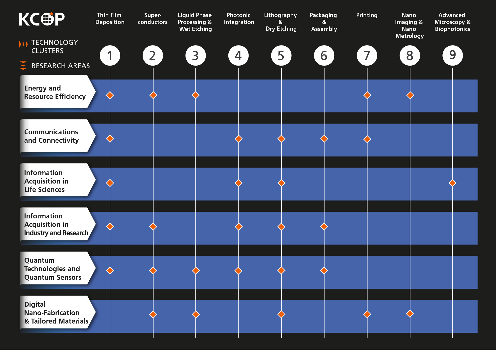
The technologies of KCOP will be organised in nine technology clusters, each comprising several laboratories. Each technology cluster is directed by an experienced staff scientist.
At KCOP we want to create a space for interdisciplinary work. For this reason several clusters are assigned to each research area.
This technology cluster is a core element of KCOP as it is the key link between the fabrication of photonic structures and photonic materials to the targeted optoelectronic applications, such as lightning devices, energy harvesting devices and teratronics.
On the one hand, the cluster will encompass a broad range of deposition systems to fabricate various types of thin-films in various environments, e.g. vacuum-based processes as well as thin-film deposition from solution in an inert atmosphere. On the other hand, this cluster involves methods to pattern photonic materials, devices and/or function layers. In this manner, the required spatial selectivity for a broad range of applications can be addressed and complex optoelectronic layer stacks can be processed.
The Functional Materials Synthesis cluster will provide materials particularly interesting for areas, including i) Photovoltaics; ii) Optical components & systems; iii) Medical technology & life sciences. There are several processes that can be realised in the Functional Materials Synthesis cluster, examples being:
- Synthesis of spectral harvesting materials, including nanosized phosphors and organic luminophores;
- Development of nonporous inorganic/organic structures for photocatalysis;
- Synthesis of photonic markers for bio applications;
- Silicon wafer processing
The chemical laboratory will play a central role in this technology cluster, with methods including synthesis under vacuum and protective atmosphere, high temperature reactions, and efficient separation and purification. The synthesis of nanomaterials will be supported by a suite of versatile material characterisation methods also focused on fundamentally understanding structural properties in order to guide and improve synthetic conditions.
The technology cluster “Photonic and Teratronic Integration” (PTI) complements KCOP’s general-purpose technology clusters Advanced Lithography, Thin-Film Deposition and Patterning and 3D Photonic Nanofabrication by offering dedicated items of equipment and work spaces needed for fabrication, characterisation, and demonstration of teratronic devices and systems. This comprises a laboratory equipped for hybrid photonic integration (Hybrid Photonic Integration Laboratory, HPI), a laboratory for 3D integration of teratronic devices and multi-chip systems (Three-Dimensional Teratronic Integration Laboratory, 3DTI), as well as an equipment and workspaces for characterisation and functional demonstration of teratronic devices and systems (Teratronic Device Characterisation and Demonstration Laboratory, TDCD). The PTI technology cluster is closely
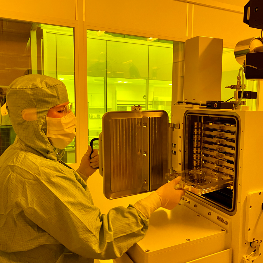
The technology cluster “Advanced Lithography” (AL) comprises high-end tools for both 2D and 3D nanofabrication. Regarding nanofabrication of planar structures, the cluster comprises electron-beam lithography tools enabling the realization of structure sizes down to 10 nm, as well as mask-based and direct-write optical lithography for fabrication of largearea structures with larger feature sizes. These lithography techniques shall be complemented by a so-called NanoFrazor system, which exploits concepts from atomic force microsopy and allows to directly structure planar surfaces with a resolution of down to 10 nm. The technology cluster will further comprise a resist laboratory containing all work space and devices needed for substrate coating (e.g. spin coater), for substrate development (e.g. spray developer) and first inspection.
Lithography of planar structures shall be complemented by tools for fabrication of truly 3D structures with micrometre and nanometre feature sizes, which is essential for a large variety of photonic devices and architectures. Examples are photonic wire bonds for connecting elements on planar optical chips, freeform microstructures for making metal contacts on solar cells or organic light-emitting diodes invisible, other 3D micro-optics, 3D optical metamaterials, and printed nano-optomechanical structures devices. The Advanced Lithography cluster makes such technologies readily available both to groups within KCOP and other external users, as well by running three state-of-the-art Nanoscribe GmbH 3D laser lithography systems and the corresponding infrastructure.
Moreover, the cluster will contain a dedicated laboratory within KCOP, in which 3D structure technologies tools are further developed. This concerns boosting the spatial resolution by exploiting new chemistries for STED-like processes, realizing -orthogonal writing modalities, and increasing the writing speed by orders of magnitude by using multiple laser beams. Furthermore, technologies for automating the alignment with respect to prefabricated planar architectures shall be brought forward.
The Detector Fabrication technology cluster will enable the production of various types of superconducting sensors and sensor prototyping. It is optimised for high through-put and yield. Sensor production is complemented by packaging and interconnect technology to produce modules and fully functional electrical, thermo-mechanical systems. The latter part is optimised to integrate sensors with custom microelectronic, photonic or electrooptical chips for numerous applications and contexts.
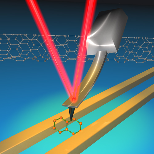
The nanocharacterisation and advanced spectroscopy cluster will provide tools for detailed fundamental characterisation of optoelectronic and photonic materials, and devices based thereon. In terms of nanocharacterisation, high resolution techniques such as advanced atomic force microscopy will play a central role in this technology cluster. This is a prerequisite for the characterisation of state-of-the-art opto-electrical and opto-photonic components. These fundamental characterisation techniques will be complemented by a suite of advanced optical spectroscopies also focused on fundamentally understanding optoelectronic and photonic materials in order to guide and improve device design. This cluster will be of importance for the design of solar cells, sensors, detectors, and photonics devices.
The challenge of understanding biological processes requires visualisation and quantification at multiple temporal and spatial scales, from single molecules up to the whole organism. In this regard, optical microscopy and spectroscopy represent key enabling technologies. For example, recent developments now enable the quantitative visualisation of single molecules in the context of a whole organism. However, these methods are still far from routine application. Therefore, a major aim for this cluster will be to establish an imaging facility, in which these state-of-the-art microscopy and spectroscopy methods will be made available for more routine use. While state-of-the-art fluorescent microscopy allows the visualisation of labelled molecules at very high resolution, other imaging modalities such as electron microscopy are required to visualise the cellular context, including organelles and the overall cellular membrane organisation. Thus, the second aim of the cluster will be to establish technology for combining multiple imaging modalities to analyse the very same sample in so-called correlative imaging. The third major aim for the cluster in the areas of microscopy and spectroscopy will be to further develop beyond state-of-the-art technology in particular in the area of nanoscale optical imaging techniques (“super-resolution imaging”, STED microscopy and localization microscopy).